
COB LED display packaging technology inventory
Catalog
Abstract: Nowadays, in the field of LED display applications, SMD and COB technologies are “equally divided” and each has accumulated a large number of loyal fans. However, in the field of tiny pitch LEDs, due to the various limitations of SMD structure, COB is becoming a mainstream technology that all major manufacturers are competing to develop.
Along with the rise of new industries such as 5G+8K and XR virtual shooting, indoor small-pitch LED displays have gradually become the first choice for high-end indoor large-screen display applications. Many manufacturers are constantly innovating the industry’s technical means to seek better small-pitch solutions in pursuit of smaller pitch and more extreme viewing effects.
Nowadays, in the field of application side, SMD and COB two technologies are “equally divided”, each accumulated a large number of loyal fans. However, in the field of tiny pitch LEDs, due to the various limitations of SMD structure, COB is becoming the mainstream technology that all major manufacturers are competing to develop in the industry.
According to the “China LED Small Pitch Market Analysis Report 2021” released by DISCIEN, China LED small pitch sales reached $2.45 billion in 2021, of which the share of COB small pitch in the P1.6 and below pitch segment grew by 3.4% year-on-year, and the share of COB products in the P1.1-P1.4 pitch segment accounted for nearly 50%. This means that COB is gradually becoming the optimal solution for tiny pitch LED display, and highlights the huge development space of COB small pitch.
1.COB vs SMD
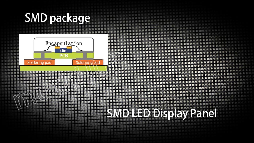
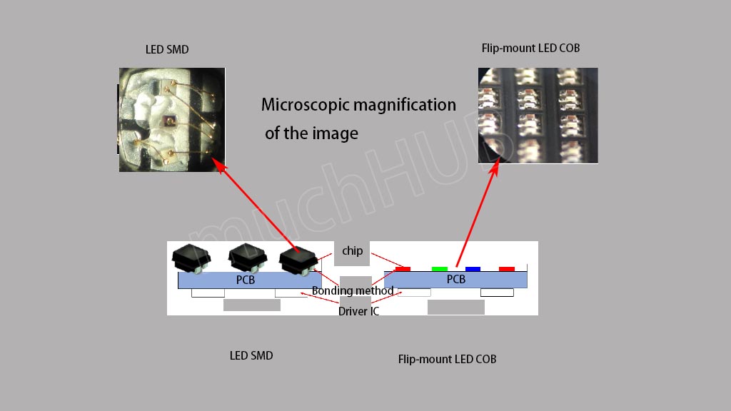
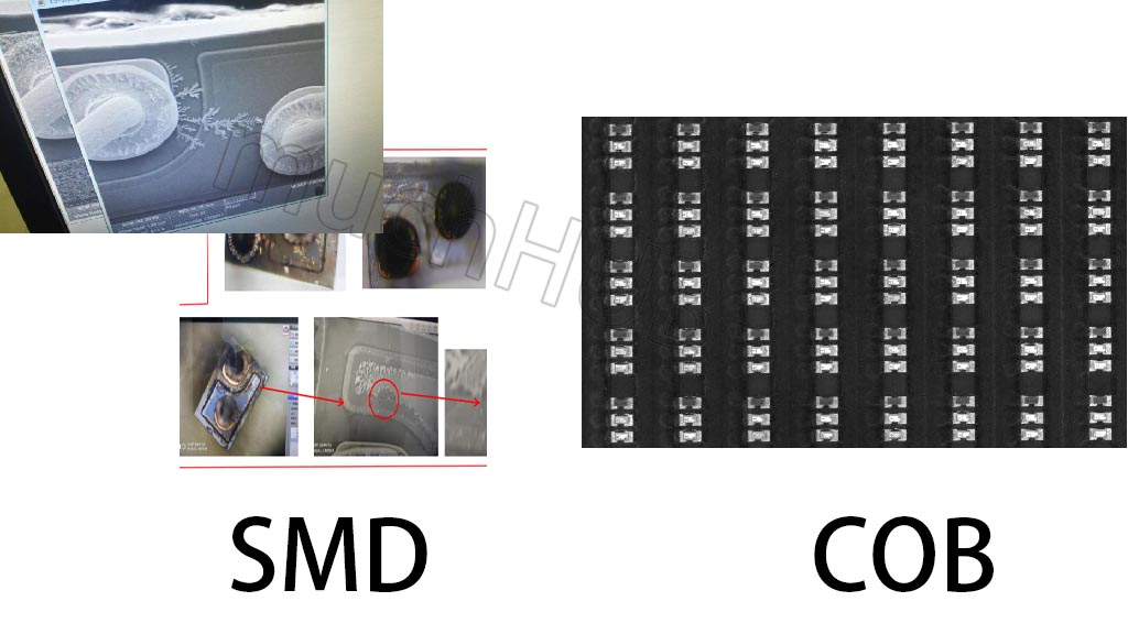
SMD, abbreviation of Surface Mounted Device, is the lamp cup, bracket, chip, lead, epoxy resin and other materials packaged into different specifications of the lamp beads, and then through the form of SMD welding on the PCB board to form the LED display module.
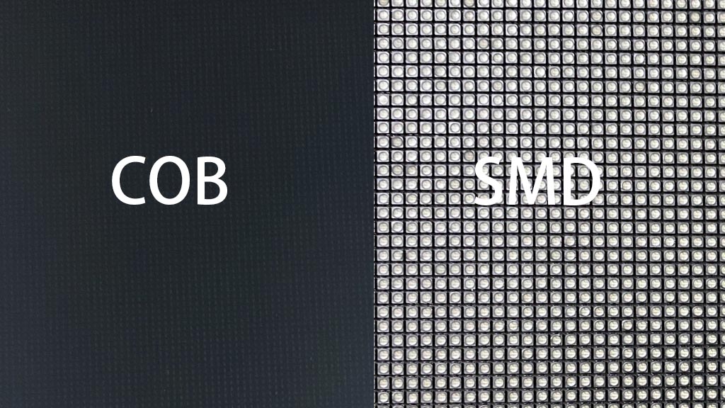
SMD LED display generally requires the LED beads to be exposed, which is not only prone to the problem of string light between pixels, but also makes the protection performance poor, affecting the imaging effect and service life.
COB packaging process is to fix the LED bare chip directly to the pad, so the heat dissipation area is relatively large compared to the traditional packaging process, the material comprehensive thermal conductivity is also high, good heat dissipation. The traditional package is to fix the LED bare chip on the pad inside the bracket, and the pad needs to transfer the heat to the PCB board indirectly through the metal pin of the bracket.
COB, an abbreviation for Chip On Board, technology refers to the LED chip directly solid crystal in the printed circuit board (i.e. PCB board) LED packaging technology, rather than a piece has been formed LED package soldered to the PCB.
This packaging method has certain advantages in terms of production and manufacturing efficiency, imaging quality, protection, and the application of small micro-pitch.

2.COB SMD performance PK
2.1 Reliability PK
COB packaging technology does not require solder wire, which can completely solve the failure of SMD due to the solder wire factor, greatly reduce the risk of failure caused by metal migration, no SMD pad exposure problem, can achieve a lower failure rate.
2.2 Contrast PK
Front-mounted or vertical structure of SMD packaging technology chip light-emitting surface occupies a small proportion of the flip COB chip area on the PCB board occupies a smaller proportion, no electrode blocking, improve the chip luminous rate, the same size of the chip higher brightness, smaller chip to achieve ultra-high contrast.
2.3 Stability PK
COB package can reduce the thermal resistance and solve the problem of heat release from sapphire or GaAs substrate; larger area of electrodes directly connected to the substrate, so that the electronic components have better heat dissipation and improve the color stability and service life of LED display.
2.4 Stability PK
SMD package display due to the surface without optical treatment, in the side viewing prone to pitting, color deviation and other phenomena; and COB technology after epoxy resin or silicone encapsulation, the surface is smooth and flat, horizontal and vertical viewing angle wide, wide color gamut, surface luminescence is not harsh, the viewing experience is more perfect.
2.5 Protection PK
The surface treatment technology adopted by COB can prevent the LED from failing to work due to water, moisture, external cuts and other damage, making the display more resistant to impact and wear, dust and moisture; frontal IP65 waterproof, anti-static, scratch-resistant, can be cleaned with water or alcohol scrubbing, so that users can use more at ease in the epidemic era. SMD display lamp beads are easy to fall off or dead light bad spots, the surface protection is weaker.

2.6 Face light source PK
With optical film technology, COB package LED display can achieve surface light source, non-blinding, short imaging distance, effectively shorten the * best viewing distance, high sharpness plus soft display, better display effect; SMD point light source imaging, close look at the pixel dot obvious, affecting the image quality.
As we can see from the above, COB technology is superior to traditional packaging technology in many aspects such as display effect, protection, stability and performance. With the expansion of production, COB manufacturing costs will certainly be popularized by the significant decline.
3.COB application prospect
Nowadays, China vigorously supports the development of ultra-high-definition video display industry, and the shipments and market share of ultra-high-definition video display terminals continue to rise globally. In the future, with the gradual sinking of LED application market, users’ requirements for display quality, stability and reliability of display products will also be higher and higher.
COB technology, with its advantages of high stability, high reliability and high display quality, has become one of the mainstream technology routes in the industry. The COB package features, which are not limited by the lamp beads and are directly encapsulated on the PCB board, make it easier to achieve high-density arrangement of light-emitting chips, and in the future, combined with the development of Mini & Micro LED technology, will more effectively promote LED display products into the era of tiny pitch.
Subscribe
Join us to learn the latest technology together
